
Windows Integrated Photonics Workspace
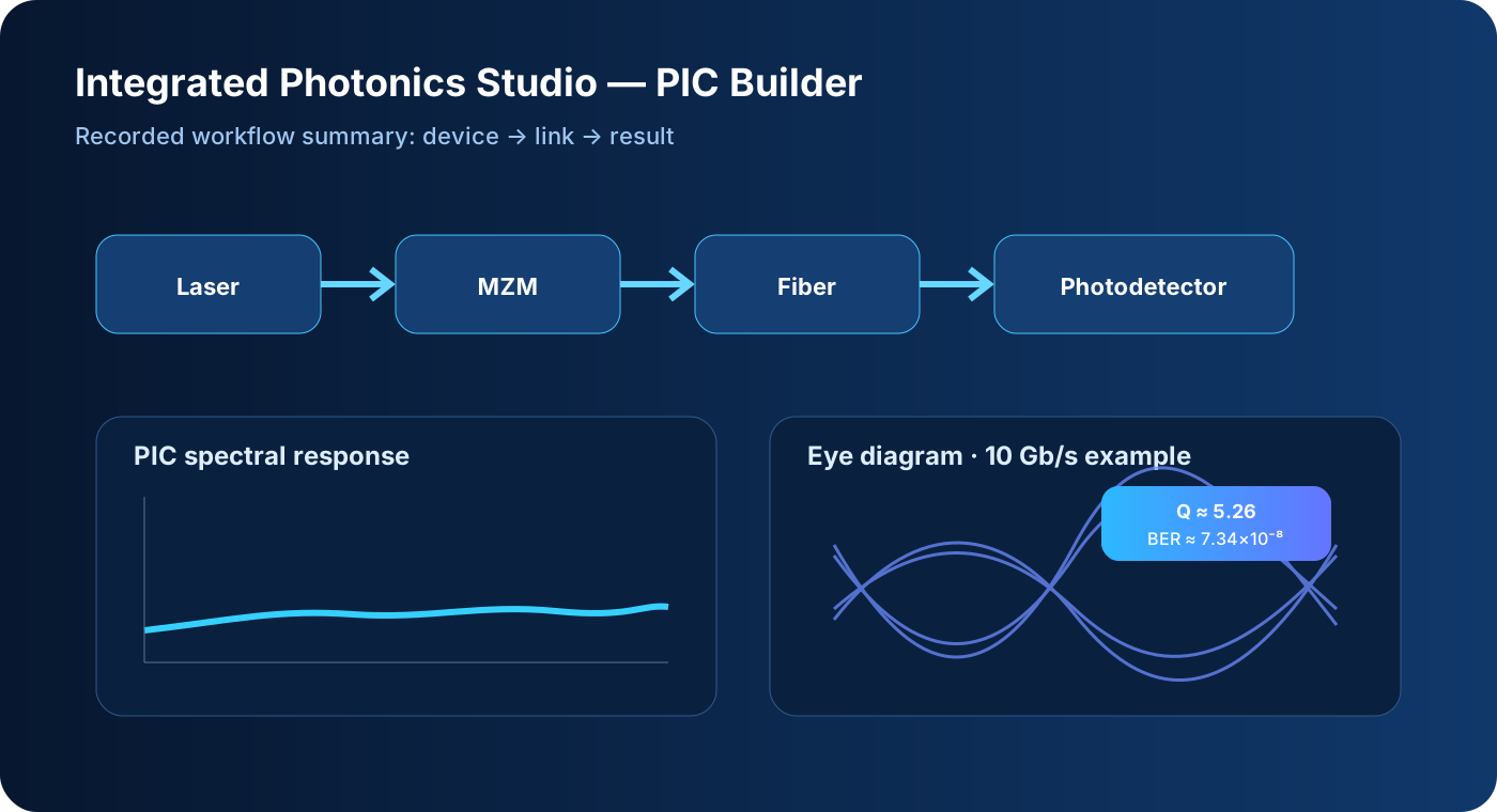
A full desktop workflow for PIC structures, device physics, optical links, DSP, tolerance, optimization and the Design Agent.
INTEGRATED PHOTONICS · WINDOWS
PIC devices → optical links → robust optimization → agent-assisted design
Build PICs, run deterministic engineering solvers, inspect link performance and compare design candidates in one Windows workspace. The Design Agent plans the workflow while numerical engineering values remain solver-generated.
PLATFORMS
Each platform is designed for a different workflow: desktop for deeper engineering analysis and mobile for portable calculations and quick checks.
A full desktop workflow for PIC structures, device physics, optical links, DSP, tolerance, optimization and the Design Agent.
CAPABILITIES
The recorded workflow is organized into four stages: Mode & Materials, Link / DSP, Tolerance & Optimize, and the Design Agent.
Build visual PICs with Laser, Waveguide, Coupler, Ring, MZM, Amplifier, Detector and related blocks.
Mode fields, effective index, dispersion, polarization, coupling, ring response and modulator characteristics.
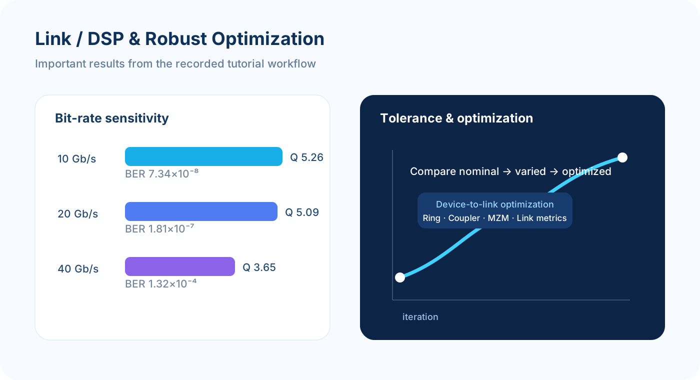
Link budget, OSNR, Q-factor, BER, eye diagrams, frequency response, coherent DSP and fiber nonlinear effects.
Fabrication variation, Monte Carlo, parameter optimization, device-to-link optimization and agent-assisted candidate comparison.
RESULTS & WORKFLOWS
Instead of a feature-only list, the page highlights link-quality and optimization results that demonstrate the workflow shown in the recording.
PRODUCT POSITIONING
For PIC, silicon photonics, TFLN, optical-device and optical-communications researchers. It supports education, research and design exploration; fabrication or commercial decisions should still use validated process data and independent verification.